System designers often find themselves battling power supply hum, noise, transients, and various perturbations wreaking havoc with low noise amplifiers, oscillators, and other sensitive devices. Many voltage regulators have excessive levels of output noise including voltage spikes from switching circuits and high flicker noise levels from unfiltered references. Ordinary three-terminal regulators will have several hundred nanovolts per root-hertz of white noise and some reference devices exceed one microvolt per root-hertz. DC to DC converters and switching regulators may have switching products ranging into the millivolt range covering a wide frequency spectrum. And many systems have offending devices that "dirty up" otherwise clean supply rails.
The traditional approach to reducing such noise products to acceptable levels could be called the "brute force" approach - a large-value inductor combined with a capacitor or a clean-up regulator inserted between the noisy regulator and load. In either case, the clean-up circuit is handling the entire load current in order to "get at" the noise. The approach described in this paper uses a bit of finesse to remove the undesired noise without directly handling the supply's high current.
The key to understanding the "finesse" approach is to realize that the noise voltage is many orders of magnitude below the regulated voltage, even when integrated over a fairly wide bandwidth. For example, a 10 volt regulator might exhibit 10 uV of noise in a 10 kHz bandwidth - six orders of magnitude below 10 volts. Naturally, the noise current that flows in a resistive load due to this noise voltage is also six orders of magnitude below the DC. By adding a tiny resistor, R, in series with the output of the regulator and assuming that a circuit somehow manages to reduce the noise voltage at the load to zero, the noise current from the regulator may be calculated as Vn/R. If the resistor is 1 ohm then, in this example, the noise current will be 10uV/1ohm = 10uA - a very tiny current! If a current-sink can be designed to sink this amount of AC noise current to ground at the load, no noise current will flow in the load. By amplifying the noise with an inverting transconductance amplifier with the right amount of gain, the required current sink may be realized. The required transconductance is simply -1/R where R is the tiny series resistor.
Consider the low power version shown below which might be suitable for cleaning up the supply to a low current device. A 15 ohm resistor is inserted in series with the regulator's output giving a 300 millivolt drop when the load draws 12 mA - typical for a low-noise preamplifier or oscillator circuit. The single transistor amplifier has an emitter resistor which combines with the emitter diode's resistance to give a value near 15 ohms. The regulator's noise voltage appears across this resistance so the noise current is shunted to ground through the transistor's collector. The noise reduction can be over 20dB without trimming the resistor values and the intrinsic noise of the MPSA18 is only a few nanovolt per root-hertz. Trimming the emitter resistor can achieve noise reduction greater than 40 dB as seen in the simulation where 11 ohms is about perfect.
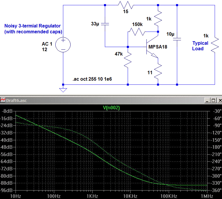
The plot above shows the rejection of noise from the noisy regulator. Even only 20 dB of rejection turns a noisy 300 nV regulator into a respectable 30 nV circuit.
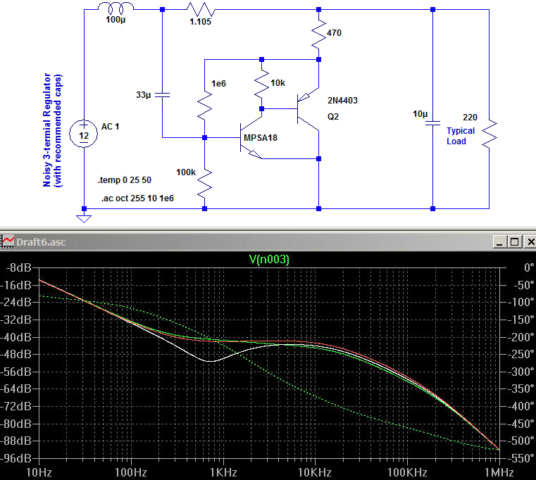
For higher current loads it is desirable to have a much lower series resistor. For such applications more gain is needed and one approach is to replace the single transistor above with a compound transistor as shown below. The effective emitter resistance is on the order of 1 ohm so a series-pass resistor near 1 ohm is just about right. The circuit is biased with a bit more current by the 470 ohm resistor and it can handle 10mV glitches of either polarity. Note there is no emitter resistance and the tweaking is done by adjusting the series resistor (shown near the optimum value of 1.105 ohms). In practice that resistor could be tweaked for best performance. I plotted the response for three temperatures, 0, 25 and 50 C, to verify that the circuit isn't particularly sensitive to temperature. The 100 uH power choke helps at the high frequency end.
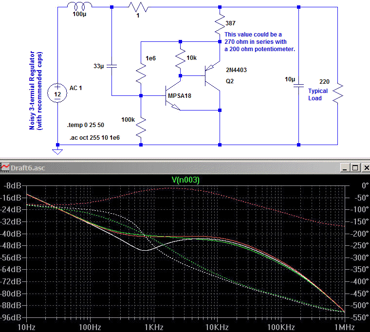
One can use a one ohm resistor for the series value and adjust the collector current in the transistor to optimize. Changing the collector (and thus emitter) current changes the emitter diode's dynamic resistance. The circuit above works well with 1 ohm for the 1.105 ohm and a 387 ohm collector instead of 470 ohm (see below). A 200 ohm pot in series with a 270 ohm resistor would give the ability to tweak the circuit:
The simplicity of the one-transistor circuit is attractive and it is interesting to investigate the possibility of using this circuit for higher currents. One limiting factor is the intrinsic resistance of the emitter that limits the gain of the single stage. Choose a large die device or a device rated for high collector current. A power transistor is a good choice even though the power dissipation will be low. The emitter resistor in the first schematic is set to zero and the bias resistor is reduced to about 5 or 10k. The collector resistor is selected to achieve the desired gain: as this resistor drops in value, the emitter resistance drops by about .025 / Ic, not including the intrinsic resistance. A 2N5192 with a 270 ohm collector resistor and a 4.7k bias resistor will work well with a 1 ohm current sense resistor and will consume about 40mA. Using a darlington for the PNP in the two-transistor version yields an emitter resistance of only 0.25 ohms.
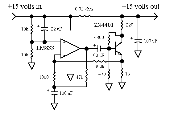
Op-amps will allow much lower series resistance. The following circuit is designed for filtering 15 volt supplies like those typically found in instrumentation. The shunt will greatly reduce white noise, spurious signals, and line-related signals on the power supply; the attenuation can exceed 40 dB with careful construction. The values are not critical except that the gain of the amplifier should be very near the ratio of the transistor emitter resistor to the series shunt resistor. In this case the gain is 15/0.05 = 300. Actually the gain is 301 with the indicated values so a 299k resistor would be theoretically better but the resistor tolerances and the actual resistance in the 0.05 ohm shunt path will cause more variation. One of the gain resistors may be made variable to allow the performance to be tweaked for the deepest null, if desired. Choose a low noise metal foil or wirewound potentiometer for best results. Standard fixed values will give excellent noise reduction sufficient for most applications. The LM833 is an excellent choice but many other low noise op-amps will work well. Choose an op-amp with a high bandwidth and low input noise voltage. A higher value shunt resistor may be used if the voltage drop can be tolerated; adjust the gain of the amplifier to match as described above. The LM833 is a dual op-amp so two shunts may be implemented with the one package for filtering two different supplies or for cascading two shunts for additional line rejection and noise reduction. The noise shunt provides no load rejection beyond the rejection provided by the source regulator through the 0.05 ohm resistor.
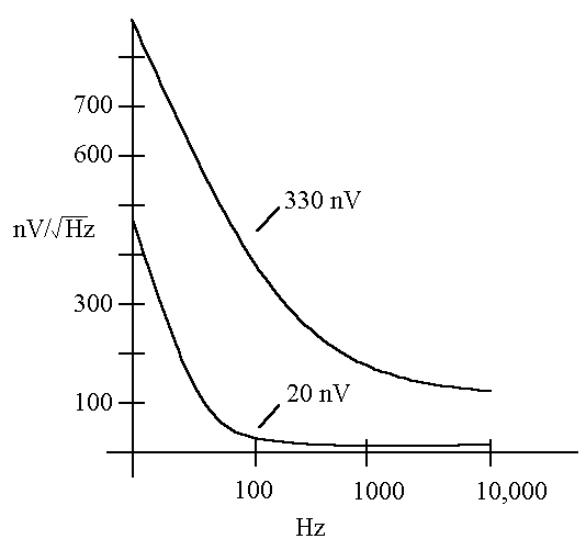
The following graph shows the performance of the noise shunt when powered by a three-terminal regulator. The regulator's noise is 330 nV per root-hertz at 100 hertz and the circuit reduces this noise to 20 nV. This 24 dB reduction is achieved without any selected values and with no particular attention paid to the layout. The one potential problem area is the grounding; heavy ground traces or even ground plane are recommended. The ultimate rejection of the circuit is better than the apparent rejection in the plot; low frequency performance is impacted by the size of the coupling capacitors and the noise floor is limited by the performance of the LM833 and resistor noise.