Micro Power
Transmitting Station
By: Richard de los Santos
Jack Dofelmire
Phong Nguyen
For: Professor Fred Williams
ECT Final Project
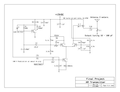
Figure
1: Schematic of the AM transmitter
Figure 2: The PCB layout for the
AM transmitter and Field strength meter
Figure 3: Schematic of the field
strength meter (Courtesy Charles Wenzel)
Table 1: Parts and prices
list for project
Figure 4: Printed Circuit Board
from PCB Express
Figure 5: Front and side views
of the AM transmitter
Figure 7: Upper and lower
sidebands with carrier in middle of scope
Figure 8: Expected tuned circuit
values. (Courtesy Charles Wenzel)
The purpose of this report is to provide background and findings or our senior project. We will discuss four steps that we used to complete our final project. The four steps of our project were research and development, design, construction, and test & acceptance. Building an AM transmitter allowed our group to apply our circuit design, fabrication skills, logical troubleshooting practices, and to prove theory of operation. It is our intent to show the step by step process of how to build and operate a micro power AM transmitter station. When you have read our report, our findings will show that this project was more than throwing parts on to a circuit board. We will show how, what, why, and when as directed by the instructor and give reason and understanding to our approach. Anyone that reads this report will gain the knowledge of how to design and implement a totally legal micro power AM transmitter station.
We decided on a micro power transmitter station because it allowed us to utilize all the skills that we have acquired attending Devry University. We had many labs throughout our studies exploring the principles and theories behind digital and analog devices. We wanted to construct a project that incorporated several key elements of our electronics program. For this project we would implement a component level construction that we would improve through test and acceptance to an industry standard following guidelines mandated by the FCC. With an improved design and a little patience, we would able to produce a very useful device that could be set up to broadcast any message of the operator’s choice or music to a small receiving area. The exact requirements to classify our project as a micro power transmitter station.
Our team was formed because of our mutual experiences in other labs throughout our degree. The first meeting was used to decide on a project that we would mutually enjoy but yet challenge our new skills. After hours of combing the Internet, we came up with several different proposals. The design that we all agreed on was and AM transmitter with an additional useful tool to be used in conjunction called a strength meter. With very helpful design ideas obtained from www.techlib.com, we began calling different manufacturers of the parts we would need to complete the project. Our first decision was finding a usable frequency that we would be transmitting our broadcast on. Our decision was on a carrier frequency of 1.64 Megahertz, because it was very available and not close to any major broadcasting stations. We called 3 different manufactures of crystal oscillators, but were discouraged by either the prices or the length of time we would have to wait for manufacturing and shipping. After several trips to a local electronics supply store, Supertronics, we decided on a lower frequency of 960 kilohertz. Although there is a major broadcasting station, KJR 950, nearby we are isolated by the shielding of the school from outside interferences. With our project decisions and task planned for each member of the team, we were on our way to designing the project.
We had our design in hand after the research and development phase of the project. In week 2 of the semester we began looking for available programs to use to put our project on the computer. We felt it was imperative to simulate our idea using multisim or a comparable program at first. After several attempts we found that our transmitter, with its very particular operation, did not simulate very well on the computer. We decided to take an inventory of the parts that we already had in our school toolbox and found that we would need to buy the majority of the parts. The team decided to put the circuit on a protoboard where we could get a rough idea of how well it would operate. Several key components such as high output transistors and the pot core were special ordered on the internet. While we waited for the delivery we set out to do a professional design and created our circuit using PCB Express. This program allowed us to design a functional layout and then we integrated that design with a spice list to a printed circuit board template. In figures 1 you see logical diagram and in figure 2 you see our final printed circuit board layout.

Figure
1: Schematic of the AM transmitter.

Figure
2: The PCB layout for the AM transmitter and Field strength meter.
The second design in our project was for a field strength meter to test our transmission from the AM transmitter. This device runs off of a 9V battery and assist the operator of the micro power transmitter station to tune for the best possible signal output. In a larger scale operation, the meter could be used near the base of a large antenna to prove transmission from an antenna. For our purpose, we were able to tune our transmitter to .1 Watt and monitor changes on the meter for maximum strength levels. It is a unique device in that it uses relatively no power unless it detects a carrier signal from the transmitter. The original device was not designed with an on and off switch to prevent operation when not needed. We did not want to drain the 9 volt battery so we just implemented one in to the design. The device operates as a small signal is received at the antenna and goes to the base of the transistor and conducts forcing the circuit in to operation. The device is sensitive to very small voltages, which makes it ideal for our purposes. The circuit then displays the incoming signal to a meter in the micro-volts range. Figure 3 is the logical diagram for the field strength meter and the PCB layout is on figure 2.
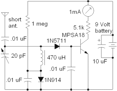
Figure
3: Schematic of the field strength meter (Courtesy Charles Wenzel)
Week five and we had our design in hand and we began the process of getting our circuit together. The parts list for both the transmitter and the strength meter was completed and the money was coming out of the pockets. We constructed the circuit as complete as we could and set week seven as the field trip day to the store to pick up the parts to finish the rest of the circuits. We wanted to build the transmitter as soon as possible incase we had any problems with our circuit. We did end up settling for a 960 kHz crystal because of cost and convenience. Later we found that it is less of a performer than we wanted, but it did serve the function that it was intended for.
| AM
Transmitter |
QTY |
Price |
Total
3 Systems |
For
3 Systems |
| broadcast
band Crystal |
1 |
$3.67
|
3 |
$11.01
|
| 10k
resistor |
1 |
$0.00
|
3 |
$0.00
|
| 10
microfarad |
2 |
$0.00
|
6 |
$0.00
|
| .1 microfarad |
2 |
$0.00
|
6 |
$0.00
|
| pot
core 250AL |
1 |
$2.50
|
3 |
$7.50
|
| 10
- 100 pf variable capacitor |
1 |
$2.22
|
3 |
$6.66
|
| 560
pf capacitor |
1 |
$0.97
|
3 |
$2.91
|
| 2N4401
transistors |
4 |
$0.86
|
12 |
$10.32
|
| 22
ohm resistor |
1 |
$0.10
|
3 |
$0.30
|
| 5.1
kohm resistors |
2 |
$0.00
|
6 |
$0.00
|
| 27
pf capacitor |
1 |
$0.99
|
3 |
$2.97
|
| 56
pf capacitor |
1 |
$0.79
|
3 |
$2.37
|
| .01
pf capacitor |
1 |
$0.00
|
3 |
$0.00
|
| 120
pf capacitor |
1 |
$0.78
|
3 |
$2.34
|
| 3.3k
ohm resistors |
3 |
$0.00
|
9 |
$0.00
|
| 15k
ohm resistor |
1 |
$0.00
|
3 |
$0.00
|
| 100
ohm resistor |
1 |
$0.00
|
3 |
$0.00
|
| Enclosure
Case |
1 |
$5.64
|
3 |
$16.92
|
| PCB
From PCB Express |
1 |
$20.00
|
3 |
$60.00
|
| Terminals
+ and - |
1 |
$2.00
|
3 |
$6.00
|
| TOTALS |
|
$40.52
|
|
$129.30
|
|
|
|
|
|
| Strength
Meter |
QTY |
Price |
Total
3 Systems |
For
3 Systems |
| Meg
ohm resistor |
1 |
$0.00
|
3 |
$0.00
|
| .01
microfarad capacitors |
3 |
$0.00
|
9 |
$0.00
|
| 20
pf variable capacitor |
1 |
$0.79
|
3 |
$2.37
|
| 10
microfarad cap |
1 |
$0.00
|
3 |
$0.00
|
| milliamp
analog current meter |
1 |
$15.00
|
3 |
$45.00
|
| 5.1kohm
resistor |
1 |
$0.00
|
3 |
$0.00
|
| 9V
battery |
1 |
$1.29
|
3 |
$3.87
|
| 470
microhenry inductor |
1 |
$0.00
|
3 |
$0.00
|
| 1N914
diode |
1 |
$0.63
|
3 |
$1.89
|
| Enclosure
Case |
1 |
$5.64
|
3 |
$16.92
|
| 1N5711
diode |
1 |
$0.79
|
3 |
$2.37
|
| MPSA
18 transistor |
1 |
$2.19
|
3 |
$6.57
|
| short
antenna |
1 |
$3.00
|
3 |
$9.00
|
| TOTALS |
|
$29.33
|
|
$87.99
|
Table
1: Parts and prices list for project.
We found that we had to do some cross referencing and a little research to get comparable parts that were not available through either Supertronix or Frys Electronics. Fortunately with the assistance of the people at Supertronix and Mr. Charles Wenzle, the person we obtained the idea for our project from, we were able to get everything but the special order items.
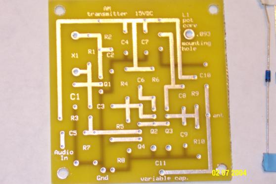
Figure
4: Printed Circuit Board from PCB Express.
After a winter break we came back with the construction process going in to full swing. We met and reviewed the design of our board on the cad software, carefully analyzing every connection before we ordered it. We decided to increase the size of the traces for ease of soldering when we put it together. We tested the circuit out on the proto board and were quite satisfied with our project. Ounce we received our boards back in a lightning fast 7 days, We soldered the components to the board and tested it with improved results, which we attribute to the fact that the proto board is not the best thing to use with a circuit of this type. We customized our project enclosure with power jacks, audio input jack, and a sleek low profile case. We soldered all of the internal connections from these jacks to the board and our transmitter was basically complete. We calculated the wave length of our antenna as follows:
Speed of light 300,000,000 divided by the frequency 960,000 Hz = Wavelength of 312.5m,
Of course per the FCC (http://www.fcc.gov/fcc-bin/assemble?docno=910724) we are limited to less than 10 ft and 100mw from our antenna, so we were not going to set any distance records. We constructed our antenna out of simple wire that was included in our tool kits from previous classes. We input a 1 kHz signal in to the transmitter at 2Vpp from the function generator and the transmission signal was 4Vpp just as we predicted. In this circuit, the final radio frequency stage is the transistor connected to the output tank. This transistor conducts one-half of the bias current flowing through the modulator transistor which is set to 20 ma. This current may be determined by measuring the voltage across the source and the 100 ohm resistor on the board. The output transistor drops about two-thirds of the power supply voltage which is 10 volts with the 15 volt supply. The power dissipated in the output stage is therefore 10ma X 10 volts which is the legal limit of 100 mw.
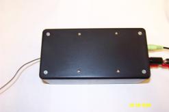
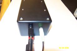
Figure
5: Front and side views of the AM transmitter.
After the project was assembled we ran audio checks with multiple sources. The first was a quick check from the CD player on one of the lab computers and it sounded great. We then connected the output of the antenna to an oscilloscope and took measurements making sure we had amplitude modulation with little or no over modulation. At 2Vpp input, which is what the circuit is designed for, we achieved 4Vpp out, exactly what we expected.
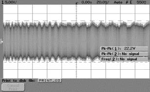
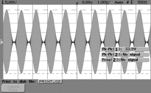
We did find, through trial and error, that as the voltage driving the circuit decreased, we had significant audio increase. The problem was that that as we came down from 15 Volts the circuit modulation was impaired greatly. We also found that an audio input more or less than 2Vpp did not drive the transmitter to overcome surrounding radio stations. We would here hums and interference from almost anything. We found this out by using a small MP3 play that’s output was 300mv and later in testing the circuit with slightly higher values from the function generator. Our conclusion was that the limiting circuitry built in to the systems keeps it from modulating more that 100mw. As you can see in the diagram above on the right, perfect modulation only occurred at the 2Vpp point. Music still sounded fine, but 100% modulation cleared up any interference from lights or surrounding electrical devices.
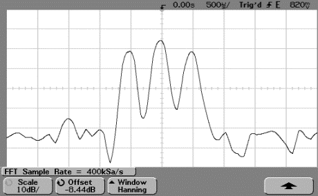
Figure
7: Upper and lower sidebands with carrier in middle of scope.
We measured a frequency of 961 KHz at the oscilloscope and everything seemed to be right on specifications for our project. We took more readings and then called the micro powered transmission station complete. We put the field strength meter close to the antenna and adjusted the variable capacitor for a max reading and when turned on, the meter registered signal levels. When music was played through the transmitter we monitored the fluctuations on the strength meter to the beat of the music, proving that the output signal was the driving force behind the meters readings. For a maximum output on our project, it would have been more advantages to use a 1.6 – 1.68 MHz crystal oscillator. From the chart below you will see justification of this theory.
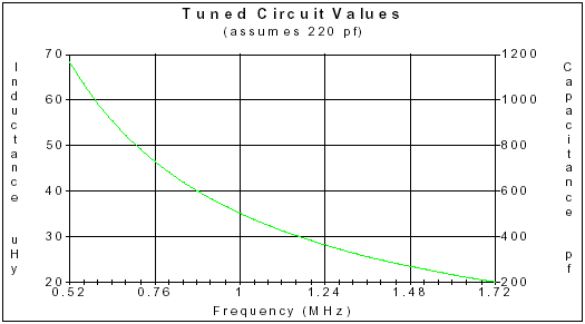
Figure
8: Expected tuned circuit values. (Courtesy Charles Wenzel)
At a higher range of frequency in the normal AM band, the circuit is near complete tuning and in our range of 960 kHz we had room for improvement. Our range is limited only by the frequency that we used and the fact that a major radio station is nearby.
Already seen on the road today are signs saying tune to this frequency for road hazards and traffic warnings. This is accomplished by a similar device with a little more range.
We envisioned using this transmitter as a way of telling your kids to come home from playing outside by sending an alarm signal or voice to small radios on their bikes.
A baby monitors could be set up with a microphone to the transmitter and listen to a radio in another part of the house.
Transmitting very low speed data signals over the air could also be achieved with a little stronger output and additional equipment.
A bugging device, although not exactly ethical, could also be set up.
Whatever application you use this for; it appears to be very durable, it is built for safety, and it has proven itself as being very reliable. There is very little power consumption and it can be run off of batteries if need be. We call our project a success because of 3 key elements.
It sounds much like an audition for an employment opportunity, and maybe it is, but that is why we endeavored to succeed at Devry.
We would
like to thank Mr. Charles Wenzel for his assistance in getting some key parts and for his
encouragement. Several of the diagrams in
this report are Courtesy of him and reflect his true enthusiasm in helping other radio
hobbyist.
http://www.calcrystal.com/. “Your Source for Crystals and Clock Oscillators” 10 February 2004.
http://www.fcc.gov/fcc-bin/assemble?docno=910724. “FCC USA” 10 February 2004.
https://www.techlib.com/electronics/amxmit.htm. “Personal Radio Station” 10 February 2004.